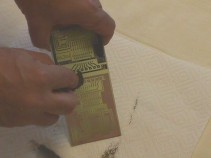
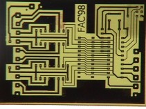
Press n Peel (PnP) Blue metal Etching Transfer Paper allows high quality Metal parts for Jewellery making and PCBs resist layouts to be rapidly produced making your design ready to etch, removing the need for UV exposure and Developing chemicals. PnP Blue is a Mylar (Polyester) backed material in which several layers of release agents and resist coatings are applied. An image is printed or photocopied onto this film, using any standard laser printer or photocopier (Dry toner based), and subsequently the Press n Peel film is ironed, laminated or heat pressed onto a cleaned copper clad board. The material will work with many different types of metal inclding Silver, Copper and stainless steel etc.
The image print area applied to the film is subsequently transferred to the copper clad laminate circuit board, along with the high quality resist (blue). The film is then removed and the resulting board is ready to etch in Ferric Chloride.
The Steps for processing are:-
1.Photocopy or Laser Print circuit image onto the dull side (emulsion) of Press-n-Peel Image Transfer Film. Prepare: Clothes, Copper Scrub Cleaning Block (Part no PCB-SCRUB) Heat Press/Laminator/Iron, Packaging Tape,Photocopy or Laser Printed Circuit Image, & Directions
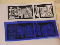
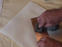
2.Cut Press-n-Peel, leaving a 1/4″ border around the circuit image. Cut board to size using a Fortex PCB shear, Clean copper board with Copper Scrub Cleaning Block (Part no PCB-SCRUB). Rinse cleaned board with soap and water. Be sure to remove all soap residue. Dry thoroughly with lint-free cloth. Be sure to scrape any burrs that appear on the edge of the board that may have resulted from the cutting/shearing process. Burrs tend to keep the iron from making solid contact with the Press-n-Peel Film.
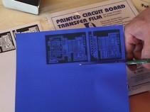
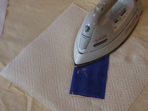
3.Place Press-n-Peel with image face down onto clean copper board. Use a Fortex Sheet Laminator/Heat Press or household Iron to bond the Press-n-Peel Film to the board. Use a peice of plain paper between the iron and the film to reduce friction. Temperature setting is critical, and dependant upon your laser printer or photocopier. Suggested starting temperature is 275-325 degrees F.
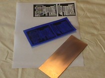
4. Quench the circuit board/Film combination under cold running water. Peel the film off. To remove small “Fills” in between traces and “Filled Donuts” cover the imaged board with adhesive tape and then remove. This should pull all filled areas away from the circuit board.
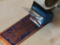
5. After removing “fills”, trim the board (if necessary) using a Fortex PCB shear to the final size. Wash the PCB circuit board in soap & water before etching to remove surface oxidisation . Etch with a suitable Etchant such as Fine Etch Crystals, Ferric Chloride or Ferric nitrate.
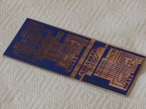
6. Using steel wool, scrub the Press-n-Peel image off to reveal copper traces. This is best done under running water. Suggestion: Do not do this until you are ready to drill and populate the board. The Press-n-Peel transfer resist protects the circuit board from oxidisation.
