Printing
Inkjet Conductive & Insulating Inks

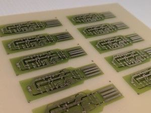
SV2 can inkjet print low-resistivity conductive inks and dielectric insulating inks to make Printed Circuit Boards (PCBs) in minutes on a variety of stiff and flexible substrates.
SV2 sequentially prints conductive traces and insulating layers, building vias in the dielectric layer to interconnect layers. Up to 6 layers can be printed, additional layers are possible at extra cost.
Specifications
| Print Technology | Thermal Inkjet Printing |
| Number of Inkjet Nozzles | 300 |
| Ink Types (curing method) | Conductive (heat), Insulating (UV) Each printed layer is 3-5 micrometers thick. Standard practice involves 9 passes, resulting in roughly 40 microns total thickness per layer. Layers can be increased in thickness up to 200 microns if necessary. |
| Min. Trace Width | 8 mils [200 microns] |
| Min. Pin Pitch | SV2 – Starter: 24 mil [600 microns] SV2 – Enhanced: 20 mil [500 microns] SV2 – Professional: 16 mil [400 microns] |
| Min. Via Dimension | Diameter: 25 mil [600 microns] Drill Size: 15 mil [400 microns] |
| Max. Printable Area | 4.6″ x 6″ [117 x 152 mm] [X/Y] |
| Conductive Ink Sheet Resistance | 40 mOhms/square |
| Number of Layers | 2 Layers SV2 Starter 4 Layers SV2 Enhanced 6 Layers SV2 Professional |
| Part attachment | We recommend using our strong conductive epoxy. Soldering using the copper PCB rivet tool (sold seperately) |
| Supported Formats | GERBER RS-274X, . jpg, .png, .tiff, .bmp |
Dispensing
Extrude conductive glues or solder pastes

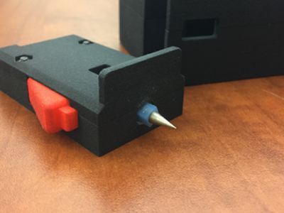
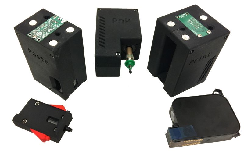
Lay down conductive glue or solder paste on printed or pre-fab boards in minutes using the Paste head.
SV2 takes eyesight and shaky hands out of the equation by precisely depositing on every pad.
Specifications
| Paste Technology | Syringe Extrusion |
| Paste Types | Conductive Epoxy and Solder Paste |
| Extruded Dot Size | 8 mils [200 microns] |
| Curing Method | Heat |
| Supported Formats | GERBER RS-274X, . jpg, .png, .tiff, .bmp |
Assembly
Extrude conductive glues or solder pastes

Printed Circuit Board Assembly (PCBA) can consume up to 80% of the entire cost of manufacturing an assembled PCB. In addition, a long back-and-forth can be required with the fab house to make sure they can source and place the parts.
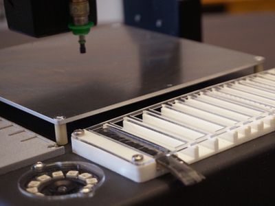
SV2 can pick-and-place components to rapidly assemble your board, using multiple vacuum tips that are automatically interchanged. SV2 also uses a camera and computer vision to make adjustments and place the parts precisely.
Finally the SV2 uses its in built heater to reflow and or cure the solder paste/glue to fix the components into please giving a fully functional working PCB.
Specifications
| PNP Technology | Vacuum Pickup, Computer Vision, Automatic Tip Swap |
| Camera | 5 MP, Upward Facing |
| Tray: Types | Tape, Individual components |
| Tape Tray: Number of Slots x Tape Width | 6 x 8mm tapes, 2 x 12mm, 1 x 16mm Cut Tapes |
| Tray: Parts loaded | Max. 42 per batch |
| Min. Part Size | 0603 [1608 Metric] |
| Max. Part Size | 0.78” x 0.78” [20 x 20 mm] |
| Supported Formats | Centroid file (text file describing Reference Designator, Footprint, X/Y location, and Rotation). The file can be generated by your CAD tool |
Pick Place Capabilities of Different SV2 Packages
SV2 Starter Pick Place Package Sizes:-
SOIC, SSOP, TSOP Type II (20-54)m TSSOP (8-38), QFP (0.8mm)
SV2 Enhanced Pick Place Package Sizes:-
SOIC, SSOP, TSOP Type II (20-86), TSOP Type 1, TSSOP (8-64), QFP (0.5mm)
SV2 Professional Pick Place Package Sizes:-
SOIC, SSOP, TSOP Type II (20-86), TSOP Type 1, TSSOP (8-80), QFP (0.4mm)

Other specifications
Mechanical
General
| Max. Substrate Size | 6″ x 6″ [152 x 152 mm] [X/Y] |
| Max. Circuit Size | 4.6″ x 6″ [117 x 152 mm] [X/Y] |
| Heads: Weight | Less than 1.1 lbs [500g] per head |
| XYZ Positioning Repeatability | ± 2.76 mil [70 microns] |
| XYZ Positioning Resolution | 0.39 mil [10 microns] |
Without the Enclosure
| Frame: Size | 16.5″ L x 14″ W x 17.5″ H [42 x 35.5 x 44.5 cm] |
| Additional Clearance Req. | 3″ [7.5 cm] in front, 4″ [10 cm] in the back |
| Frame: Weight | 30 lbs. [13.5 kg] |
| Shipping Box: Size | 21.5″ L x 17″ W x 27″ H [55 x 43.2 x 68.6 cm] |
| Shipping Box: Total Weight | 50 lbs. [22.5 kg] |
With the Enclosure
| Enclosure: Size | 24.8” L x 17” W x 18” H [63 x 43 x 46 cm] |
| Additional Clearance Req. | 6” [15 cm] on the right |
| Enclosure: Weight | 46 lbs. [21 kg] |
| Unit: Total Weight | 81.5 lbs. [37 kg] |
| Shipping Box: Size | 30” L x 28” W x 22” H [76 x 71 x 56 cm] |
| Shipping Box: Total Weight | 106 lbs. [48 kg] |
Electrical
| Power | DC 24V 22A |
| Connection | Ethernet, Wi-Fi |
Software
| Installation | None (Software runs on-board) |
| System Requirements | Web browser (Platform-independent) |
| Recommended Browser | Firefox, Chrome |
| Offline Updates | Available on demand (USB3.0) |
Compatible with Any CAD Tool
(KiCAD, Altium, Eagle, Solidworks plug-in, etc)
Export your design files from any CAD tool into GERBER, the industry standard for PCB manufacturing.
Temperature
| Ambient: Operating | 50-100F [10-40℃] |
| Heat Bed: Operating | 75-300F [25-150℃] |
| Heat Bed: Max | 340F [170℃] |
Ambient Operating Requirements
| Ambient Temperature | 50-100F [10-40℃] |
| While operating without the enclosure | Protect the work area from air flows Avoid camera exposure to direct sunlight to improve the reliability of the Computer vision |
| Other | Operation in a ventilated area recommended |


